Imaging technology
Micro CT
Nano CT
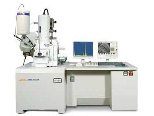
Scanning Electron Microscopy (SEM)
Transmission Electron Microscopy (TEM)
Immunoelectron Microscopy (IEM)
Cryo-Electron Microscopy (Cryo-EM)
Liquid-Phase Electron Microscopy (Liquid EM)
In Vivo Fluorescence Imaging
A scanning electron microscope (SEM) uses a very narrow electron beam to scan the sample, producing various effects through the interaction between the electron beam and the sample. The principle involves using secondary electron signals to image and observe the surface morphology of the sample. SEM is commonly used to examine the three-dimensional structures of material surfaces and cross-sections.
 Application Areas:Scanning electron microscopes (SEM) are widely used in various fields, including physics, chemistry, materials science, and biology. They are primarily employed for the observation, analysis, and testing of surface morphology and microstructures.

Hong Kong Office:224 Waterloo Road, Kowloon Tong, Hong Kong (inside the Baptist University campus)
Shanghai Office:2F, 1788 Caoyang Road, Putuo District, Shanghai
Shanghai Office:2F, 1788 Caoyang Road, Putuo District, Shanghai
copyright © ROYAL BIOTECH All rights reserved.
